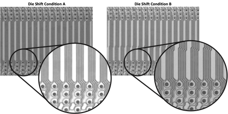
Solving the Die-Shift Problem
Rather than fight natural variation in the manufacturing process, we take a different approach: measure it and adapt. Deca’s breakthrough Adaptive Patterning (AP) technology generates a unique lithography pattern for each device on every wafer, ensuring optimal interconnect on the industry’s highest density advanced packaging.
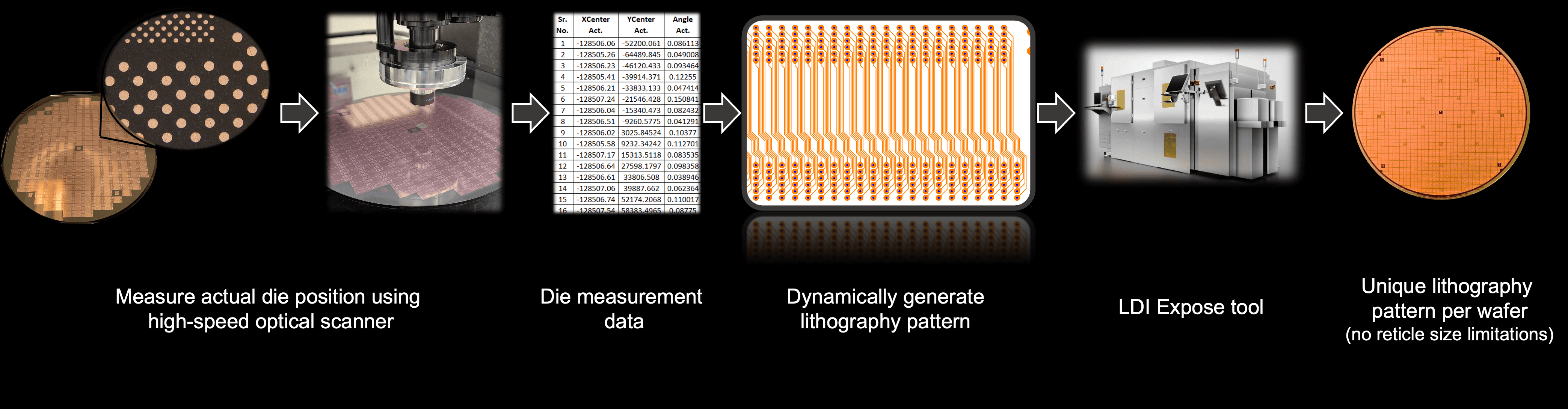
Deca’s AP technology introduces a unique approach to overcome natural variation that occurs during manufacturing. By employing real-time design-during-manufacturing (DDM) techniques, AP ensures consistent quality and performance.
The AP system utilizes a high-speed optical measurement to identify variations, allowing the AP software to rapidly generate a unique lithography pattern for each unit based on deterministic rules set by the designer. This optimized pattern is then implemented on the entire wafer or panel using a maskless Laser Direct Imaging (LDI) system, enabling precise customization for every unit.
With Adaptive Patterning, designers can scale to unprecedented device interface density with wider process windows for robust manufacturability.
It All Starts with Design
Using AP Studio alongside leading EDA tools, designers have full control over the entire range of Adaptive Patterning techniques, including:
One or more of the following techniques:
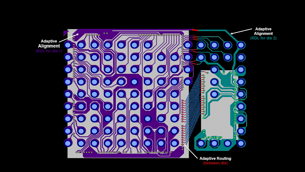
- Adaptive Alignment
- Adaptive Routing
- Adaptive Shapes
- Adaptive Metal Fill
- Adaptive Vias
- Adaptive Pad Stacks
It’s Good to be Unique – Optimize Each Device on Every Wafer
Running in the fab, Deca’s AP Engine design-during-manufacturing software generates a unique lithography pattern for each device on every wafer in real time which is then implemented using all-digital maskless lithography. With advanced laser direct imaging (LDI), millions of simultaneous, digitally-controlled laser spots scan each wafer at high throughput.
Scalable for the Future of Chiplets
Adaptive Patterning seamlessly scales from dozens of wires on an internet-of-things device to tens of thousands of wires on a leading-edge chiplet AI processor.
Adaptive Patterning Software Ecosystem
Our comprehensive software suite provides unique design capabilities, unparalleled performance in the fab, and full equipment integration to unlock the power of Adaptive Patterning.
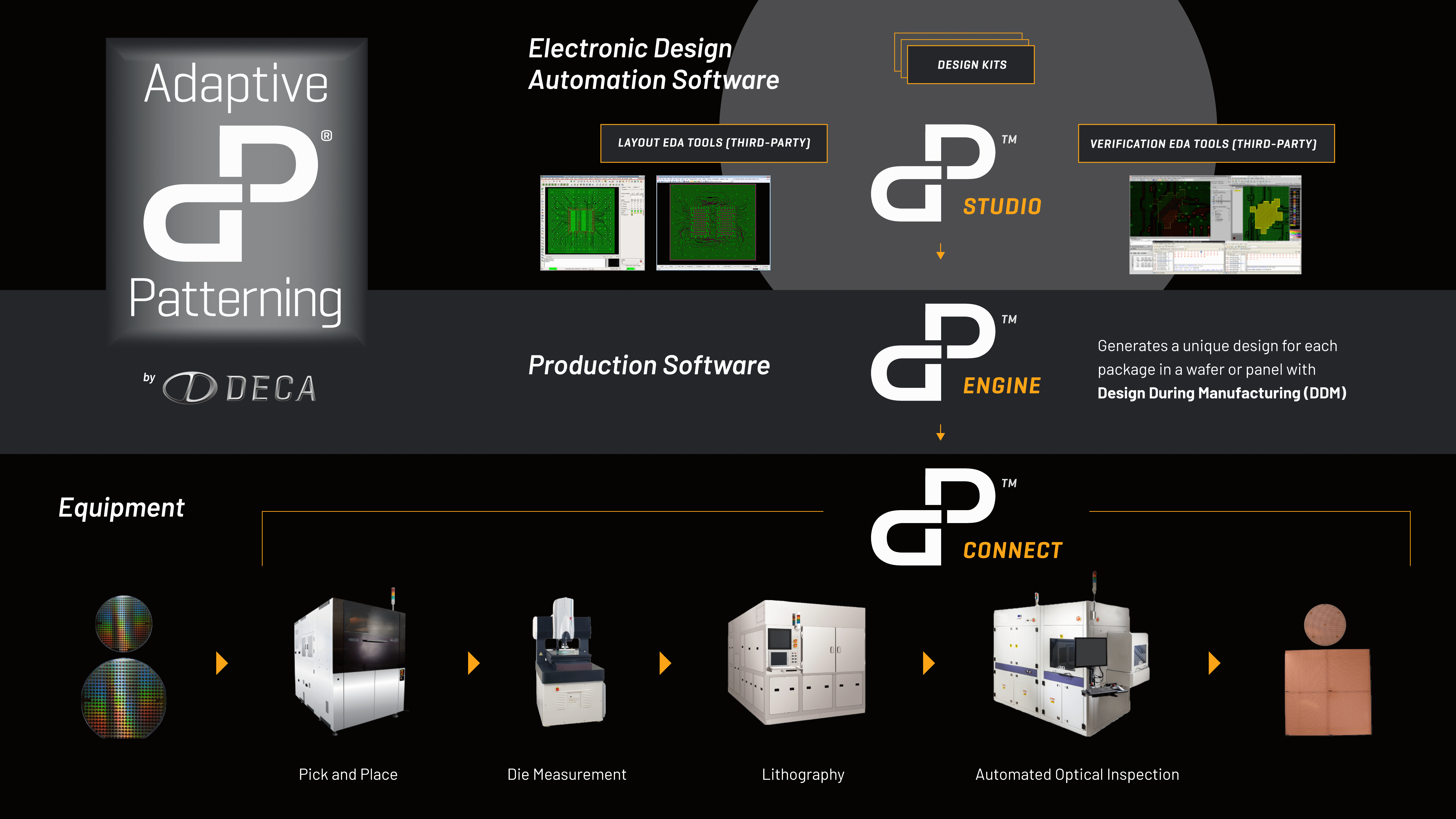
AP Studio
Our innovative design system for Adaptive Patterning, AP Studio, is integrated with industry-leading EDA tools from our partners to provide a powerful design environment that scales from chip scale packages to the most advanced chiplet-based designs. With Adaptive Patterning Design Kits (APDKs) that provide comprehensive design guides, design rules, DRC decks, and data-flow automation, designers are in full control from concept to manufacturing.
AP Engine
At the heart of Design-During-Manufacturing (DDM) is AP Engine, performing real-time design on every package as it flows through the manufacturing process. Whether implemented on-premise with dedicated servers or running in the cloud, AP Engine provides reliable and scalable execution for the fab.
AP Connect
The Adaptive Patterning ecosystem fully embraces the equipment backbone of the manufacturing process through the new AP Connect program. Leading original equipment manufacturers (OEMs) are partnering with DECA to integrate AP Connect software directly into their latest manufacturing equipment. Combined with AP Studio and AP Engine, AP Connect ensures equipment is ready for Adaptive Patterning from day one.