Over the years, Deca Technologies have developed an extensive patent portfolio focusing on three main areas of technology namely: Adaptive Patterning®, M-Series, and Autoline. These three technology areas are the pillars enabling Deca’s mission of creating advanced electronic interconnect solutions for the Chiplet Era.
Adaptive Patterning®

prestratum to the fixed prestratum
(US Patent # 8,656,333)
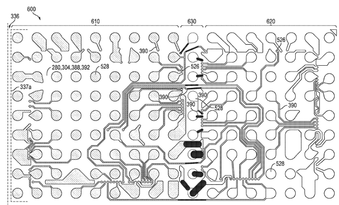
using Adaptive Alignment
(US Patent #10573601)
| 8,656,333 | Integrated Circuit Package Auto-Routing |
| 8,799,845 | Adaptive Patterning for Panelized Packaging |
| 8,826,221 | Adaptive Patterning for Panelized Packaging |
| 182715 | Adaptive Patterning for Panelized Packaging |
| 9,040,316 | Semiconductor Device and Method of Adaptive Patterning for Panelized Packaging with Dynamic Via Clip |
| 9,196,509 | Semiconductor Device and Method of Adaptive Patterning for Panelized Packaging |
| ZL 201180001658.9 | Adaptive Patterning for Panelized Packaging |
| 11201503242W | Semiconductor Device and Method Of Adaptive Patterning for Panelized Packaging |
| 9,397,069 | Semiconductor Device and Method of Adaptive Patterning for Panelized Packaging with Dynamic Via Clip |
| 9,401,313 | Automated Optical Inspection of Unit Specific Patterning |
| 9,418,905 | Adaptive Patterning for Panelized Packaging |
| 9,520,331 | Adaptive Patterning for Panelized Packaging |
| 9,520,364 | Front Side Package-Level Serialization for Packages Comprising Unique Identifiers |
| ZL 201380033254.7 | Integrated Circuit Package Auto-Routing |
| 9,818,659 | Multi-Die Package Comprising Adaptive Alignment and Routing |
| 9,887,103 | Semiconductor Device and Method of Adaptive Patterning for Panelized Packaging |
| ZL 201380064057.1 | Semiconductor Device and Method of Adaptive Patterning for Panelized Packaging |
| 10,056,304 | Automated Optical Inspection of Adaptive Patterning |
| 10,157,803 | Semiconductor Device and Method of Unit Specific Progressive Alignment |
| 10-1957851 | Semiconductor Device and Method of Adaptive Patterning for Panelized Packaging with Dynamic Via Clip |
| 10-2016-7035116 | Semiconductor Device and Method of Adaptive Patterning For Panelized Packaging with Dynamic Via Clip |
| ZL 201580033193.3 | Semiconductor Device and Method of Adaptive Patterning for Panelized Packaging with Dynamic Via Clip |
| 1674635 | Multi-Die Package Comprising Adaptive Alignment and Routing |
| 10-2081684 | Front-Side Package Level Serialization for Packages Comprising Unique Identifiers |
| 10-2081682 | Multi-Die Package Comprising Adaptive Alignment and Routing |
| 10573601 | Semiconductor Device and Method of Unit Specific Progressive Alignment |
| 9,978,655 | Semiconductor Device and Method of Adaptive Patterning for Panelized Packaging With Dynamic Via Clip |
| 6685301 | Automated Optical Inspection of Adaptive Patterning |
| 1234252 | Semiconductor Device and Method of Adaptive Patterning for Panelized Packaging with Dynamic Via Clip |
| ZL 201580045860.X | Front-Side Package Level Serialization for Packages Comprising Unique Identifiers |
| 10-2197228 | Semiconductor Device and Method of Unit Specific Progressive Alignment |
M-Series Patents
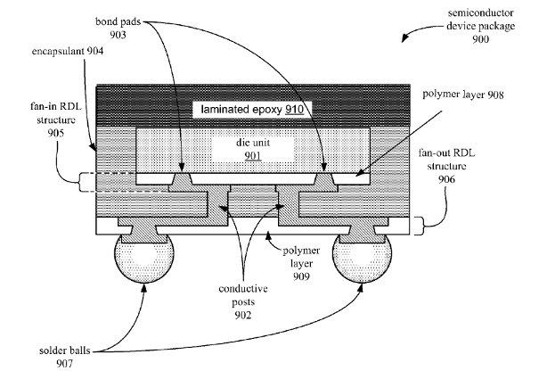
(US Patent # 8,535,978)
(US Patent # 9,502,397)
| 8,535,978 | Die Up Fully Molded Fan-Out Wafer Level Packaging | |
| 8,835,230 | Fully Molded Fan-Out (Method) | |
| 8,922,021 | Die Up Fully Molded Fan-Out Wafer Level Packaging | |
| 8,604,600 | Fully Molded Fan-Out (device) | |
| 9,177,926 | Semiconductor Device and Method Comprising Thickened Redistribution Layers | |
| ZL 201180008457.X | Fan Out Wafer Level Package with Transferred Dielectric | |
| 9,269,622 | Semiconductor Device and Method of Land Grid Array Packaging with Bussing Lines | |
| 9,337,086 | Die Up Fully Molded Fan-Out Wafer Level Packaging | |
| 11201404309V | Die Up Fully Molded Fan-Out Wafer Level Packaging | |
| 11201504442Y | Semiconductor Device and Method of Land Grid Array Packaging with Bussing Lines | |
| 9,502,397 | 3D Interconnect Component for Fully Molded Packages | |
| ZL201210311793.X | Fully Molded Fan-Out | |
| 9,576,919 | Semiconductor Device and Method Comprising Redistribution Layers | |
| 11201404307T | Fully Molded Fan-Out | |
| 9,613,830 | Fully Molded Peripheral Package on Package Device | |
| ZL 201280069322.0 | Die Up Fully Molded Fan-Out Wafer Level Packaging | |
| 9,754,835 | Semiconductor Device and Method Comprising Thickened Redistribution Layers | |
| 9,761,571 | Thermally Enhanced Fully Molded Fan-Out Module | |
| 9,831,170 | Fully Molded Miniaturized Semiconductor Module | |
| 10,050,004 | Fully Molded Peripheral Package on Package Device | |
| I643271 | Thermally Enhanced Fully Molded Fan-out Module | |
| 10201503498X | Fan Out Wafer Level Package with Transferred Dielectric Film | |
| ZL 201480008489.5 | Semiconductor Device and Method of Land Grid Array Packaging with Bussing Lines | |
| 10,373,902 B2 | Fully Molded Miniaturized Semiconductor Module | |
| 10,373,870 | Semiconductor Device and Method of Packaging | |
| 1674658 | Fully Molded Miniaturized Semiconductor Module | |
| I690044 | 3D Interconnect Component for Fully Molded Packages | |
| 10-2114563 | Thermally Enhanced Fully Molded Fan-Out Module | |
| 10,672,624 | Method of Making Fully Molded Peripheral Package on Package Device | |
| 10-2127774 | Fully Molded Miniaturized Semiconductor Module | |
| 10,720,417 | Thermally Enhanced Fully Molded Fan-Out Module | |
| 10-2164011 | Fully Molded Peripheral Package on Package Device | |
| 10-2164012 | Fully Molded Peripheral Package on Package Device | |
| 10,818,635 | Fully Molded Semiconductor Package for Power Devices and Method of Making the Same |
Autoline Patents
and two-step Rapid Cure
(US Patent # 9,159,574)
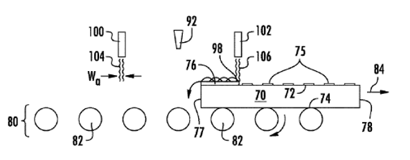
(US Patent # 9,640,495)
(US Patent # 9,464,362)
| 8,784,621 | Wafer Carrier Comprising a Variable Aperture Shield |
| 8,932,443 | Adjustable Wafer Plating Shield and Method |
| 9,159,547 | Two Step Method of Rapid Curing a Semiconductor Polymer Layer |
| 9,464,362 | Magnetically Sealed Wafer Plating Jig System and Method |
| 9,613,912 | Method of Marking a Semiconductor Package |
| 9,640,495 | Semiconductor Device Processing Method for Material Removal |
| 9,653,339 | Integrated Shielding for Wafer Plating |
| ZL201280075204.0 | Magnetically Sealed Wafer Plating Jig System and Method |
| ZL 201480051294.9 | Two Step Method of Rapid Curing a Semiconductor Polymer Layer |
| 10,204,803 | Two Step Method of Rapid Curing a Semiconductor Polymer Layer |
| I664708 | Method of Marking a Semiconductor Package |
| 10373913 | Method of Marking a Semiconductor Package |
| ZL 201580069079.6 | Method of Marking a Semiconductor Package |
| 10-2081683 | Semiconductor Device Processing Method for Material Removal |
| 10600652 | Semiconductor Device Processing Method for Material Removal |
| I692023 | Semiconductor Device Processing Method for Material Removal |
| 8,236,151 | Substrate Carrier For Wet Chemical Processing |
| 10-2197220 | Two Step Method of Rapid Curing a Semiconductor Polymer Layer |